Breakthrough in 2D Material Transfer Paves the Way for Next-Generation Electronics

Researchers at the University of Manchester have developed a technique for transferring 2D crystals with unprecedented cleanliness and uniformity, bringing us closer to the commercialization of advanced electronic devices.
In a recent article published in Nature Electronics, scientists from the University of Manchester have unveiled a groundbreaking method for transferring 2D crystals. This technique utilizes an inorganic stamp to create the cleanest and most uniform stacks of 2D materials to date. Led by Professor Roman Gorbachev, the team’s innovation holds immense promise for the future of next-generation electronics.
A Leap Forward in Material Stacking
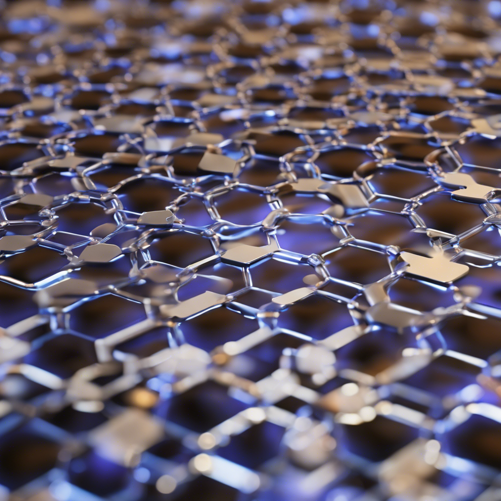
The team at the University of Manchester employed an inorganic stamp to precisely transfer 2D crystals into van der Waals heterostructures. This technique allowed for the creation of atomically clean interfaces over extended areas, surpassing the capabilities of existing methods. With this advancement, the commercialization of 2D material-based electronic devices is now within reach.
Minimizing Strain Inhomogeneity
The rigidity of the new stamp design significantly reduced strain inhomogeneity in assembled stacks. Compared to current state-of-the-art techniques, the team observed a remarkable decrease in local variation at “twisted” interfaces. This breakthrough minimizes strain-induced defects, enabling the creation of more precise and reliable electronic components.
Overcoming Surface Contamination
One of the main challenges in transferring 2D materials is surface contamination. Existing methods rely on organic polymer membranes or stamps, which introduce contaminants even in controlled cleanroom environments. The University of Manchester’s technique eliminates this issue by utilizing an ultrathin metal layer as a sticky “glue” to pick up and transfer the 2D crystals. This innovative approach ensures atomically clean interfaces, crucial for the development of industrially viable electronic components.
Enabling Designer Crystals
The precise stacking of individual 2D materials opens up the possibility of engineering designer crystals at the atomic level, resulting in unique hybrid properties. By creating flawless stacks of up to eight layers, the team’s technique allows for the construction of complex structures with precise control over the arrangement of materials. This breakthrough has the potential to revolutionize the field of materials science and advance the development of novel electronic devices.
Scalability and Real-World Applications
After successfully demonstrating the technique using microscopic flakes, the researchers scaled up the transfer process to handle larger materials grown from the gas phase. This scalability is crucial for the practical application of 2D materials in next-generation electronic devices. The ability to work with mm-scale areas provides a pathway for the integration of 2D materials into commercial products.
Conclusion:
The University of Manchester’s breakthrough in 2D material transfer represents a significant step forward in the development of next-generation electronics. By achieving atomically clean interfaces and minimizing strain inhomogeneity, this technique opens up new possibilities for the creation of designer crystals with unique properties. As researchers continue to refine and optimize this method, we can anticipate the commercialization of advanced electronic devices that harness the full potential of 2D materials.


